
FAQ
Application Products
- We offer low cost ROHS compliant PCB prototypes with Immersion gold surface finish.
- We allow multiply boards to be put on same panel.
- We will panelize many different PCB files on one panel for for additional fee, if you do the panelization yourself there will be no panelization fee..
- We will de-panelize (cut to rectangles) your boards from the panel free of charge.
- We don't charge setup, tooling, photoplots, etc you name it fees, our panel prices are all inclusive: PCB + soldermask + component print + tooling + setup + photoplots.
- We do free Design Rule Check and notify you if we find that your design violate our technological requirements or have errors.
- We produce and ship in 3-5 working days after we receive your order confirmation.
- We can ASSEMBLY your prototypes with the components we carry on stock, and it only takes extra few days.
ORDERING
We respect customer's copyright and will never manufacture PCBs for someone else with your files unless we receive written permission from you, nor we'll share these files with any other 3rd parties.
We can manufacture PCBs in any volume.
Yes, you can, but for this purpose we should receive written permission from the first customer who submitted this PCB. In this case you just have to reffer to first customer po# to re-order the PCB.
We don't investigate if the customer who submit the PCB for production is the original copyright holder, so when customer submits PCB files for manufacturing we assume he have copyright for it and the customer is responsible if he violates copyright law. Be advised that many designs made with Eagle on Internet are made with illegal Eagle licensee, so we can't open them and produce them, so before submitting Eagle design found on internet first check if it's made with legal Eagle licensee. This can be done very simple, all you have to do is to download Eagle and to run it as Freeware, then try to open the BRD file if you get "Load error" this means the Eagle BRD if made with illegal licensee and we can't manufacture.
One panel (SSS/DSS/SSQ/DSQ)
Please check if the Return-Path of your e-mail client is configured correctly. Send test e-mail to other e-mail you can verify that your e-mail client sends e-mails or check if there is not problem with your e-mail server. We respond in 24 hours, so if you don't get reply in this time please re-send your e-mail again.
PRICES
You have to check what import taxes you have to pay with your local customs authorities.
No, our web prices are export netto prices. They doesn't contain VAT.
Overlapping drill holes are not allowed to exist in your design, nor drill slots. If there are only few we'll fix (remove the duplicating drill holes) and charge you one time small amount in your po form. Please reffer to our PRICE web page for more info.
PAYMENTS
There are several ways you can pay, see below:
Card payment: we accept Visa, Eurocard, Mastercard, JCB. We can't charge Visa electron and Maestro cards, please do not send us payment forms with such cards
Paypal: we accept payments by Paypal, due to the high Paypal service charges, payments by Paypal will be subject to additional 5% service charge if your order is below EUR 100.00;
Western Union: we accept Western Union payments;
Bank transfer: we accept bank transfer payments, due to the high cost of sending and accepting bank trasnfers all orders paid by bank transfer are subject to EUR 30.00 bank handling fee if your order is below EUR 1000.00
Cheques, bankers drafts: we accept cheques and banker drafts only if they are issued by Bulgarian banks
Accounts/organization's purchase orders: We do offer Net30 credit terms to approved customers. We do not offer any other terms. To apply, email info@olimex.com, note that to have approved account one of our conditions is your purchases to be minimum EUR 1000 per month and you should have been our customer for at least six months, if you do not meet these criterias please do not apply for Net30.
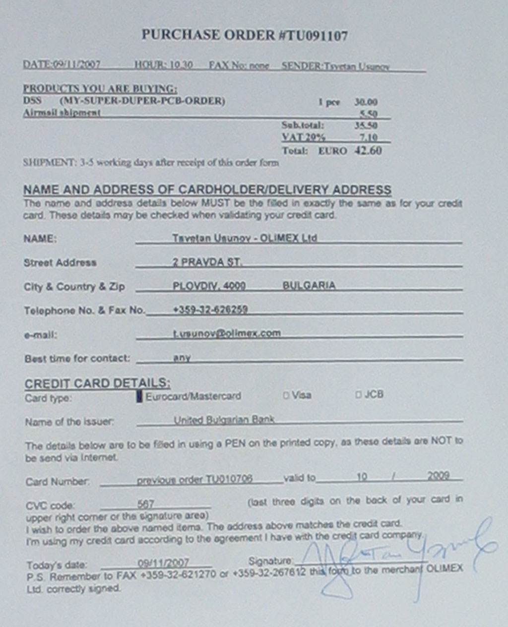
We have strict company policy for the card info. The access to this info is restricted to only few Olimex employees in our accounting where the fax numbers written on the PO form are located. The database is not on file or online but kept on paper copy only (your po form which is in our archive).
Yes you can, but if you are first time customer we must verify you are legitimate cardholder and to be sure that this is not credit card fraud attempt. For this purpose when we receive your PO form we'll first charge small random value under EUR 1.00 to your card and will wait you to report back what is the value we charged. Once you are verified as legitimate cardholder you can continue ordering from anonymous account without future verification.
No, we can't ship C.O.D.
SHIPPING
No, our price is EXW (ex-works) and doesn't include the shipping charge.
Airmail delivery is recommended parcel post service. This is post office delivery and have no tracking/tracing as Express Mail or the Courier companies.
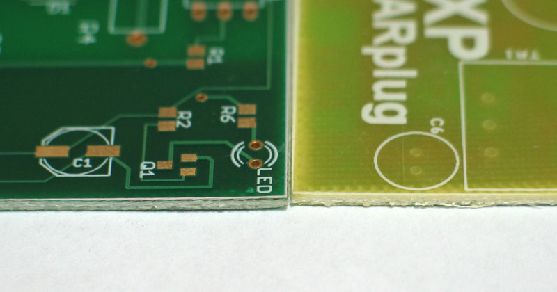
LAMINATE THICKNESS
Our standard laminate thickness is 1.5 mm (0.062")
yes we can, but we don't stock such materials, so if you want us to produce your boards on such material you have to supply the base laminates to us. Please contact us for more information how to arrange this, the panel dimensions etc.
Yes, please have look at the info below:
Laminate brand: CC-5400
Manufacturer: CKC TAIWAN
ANSI grade: FR-4
Laminate thickness 0.5 mm (0.020"), 0.8 mm (0.032"), 1.0 mm (0.040"), 1.5 mm (0.062")
copper thickness 18 um (1/2 oz) or 35 um (1 oz)
operating temperature Tg > 130 C
soldering 260C/500F - 40 sec., 290C/554F - 20 sec.
Dielectric cinstant 1Mhz: 4.0 - 4.5, guaranteed < 5.0
Dissipation factor 1MHz: 0.02-0.03, guaranteed < 0.03
Volume resistivity: Ohm.cm > 5*10^14
UL 94V-0, UL746 CTI 100
COPPER THICKNESS
We can offer 18 um (1/2 oz) and 35 um (1 oz) copper thickness.
SOLDERMASK
We use green Liquid Photo Imagable (LPI) Soldermask for our PCB production.
No, the soldermask is standard option for our prototypes, so all boards are produced with soldermask and this doesn't rise the price.
No, in matter of fact our PCB finish is immersion gold, which means if your board is manufactured without soldermask it will lead to solid gold deposit on your exposed copper area and your price will be MUCH higher than our standard panel price, if your design require absence of soldermask (RF parts, termal dessipation) please ask for special quote - we can't offer you our standard prices for PCBs without soldermask.
We print one soldermask on the copper layer of your single sided boards. It may be on top or bottom depend on where is your copper layer.
Yes, on the double sided boards we print two soldermasks on top and bottom copper layers and the soldermask may be different (SMT parts) and this doesn't involve additional charge.
COMPONENT PRINT SILKSCREEN
No the only option is white ink component print.
No, we don't check for errors nor manipulate your silkscreen, so if you component print is over your component pads you will have problems to solder your pads later. This is why we always recommend to our customers before they send their files for production to use Gerber viewer and check all their layers.
PCB SURFACE FINISH
Yes, the standard surface finish for our prototypes is Immerson Gold plating. This is Ni-Au finish over the laminate Cupper. Immersion gold and galvanic gold are the most expensive but the best ROHS compliant surface finishes on the market today.
Yes, immersion gold is most expensive, but it's the best surface finish known in the industry today. The immersion gold finish have perfect even surface and excellent solderability and outperform all other ROHS compliant alternatives like SN100C (SnCuNi) HAL or immersion Tin not speaking for the organic coating (colophone+alcohol mix) over bare copper which is worst.
The alternative pure Tin finish is cheap but suffer from these problems:
Aging: you must assembly the boards as soon as possible after the tin finish application as the solderability decreases rapidly with the time and after few months you will not be able to solder your tin coated boards tin whiskering - is very bad if your board needs to operate or be stored/transported at lower temperatures (do you know what is the temperature in the air cargo trunk?)
Poor wetting when soldering increasing the risk for poor solder joints, so you need aggresively fluxes to be used in order to make good solder joint, which then should be carefully removed as they will oxidize your solder joints if remain not well cleaned
No. We don't use SMOBC and HASL anymore, our only process now is ROHS compliant immersion gold.
DRILL HOLES
The drill tools sizes are assumed the drill tool sizes for drilling. After the plating in double side PCB the finished hole size will be -0.1 mm. i.e. 0.7 mm drill size will produce 0.6 mm final hole size. You should take this into account when you design your board. The general rule of tumb when you design your custom library parts is that if your component lead is X mm your drill hole should be X+0.3-4 mm i.e. if your component lead is 0.4 mm you must provide 0.7 - 0.8 mm drill hole, if you make the clearance bigger you will have more waste of solder when soldering and you may not fill your pads properly, if you make the clearance smaller you will have problems when you stuff your components.
No. All holes are to be plated. If you send us PCB files with split plated and non-plated holes files, the non-plated holes file will be ignored.
0.6 mm (24 mils)
5.0 mm (195 mils)
We'll not process your files and notify you that you can't use under 0.6 mm drill size in your design.
We'll replace all drill sizes over 5.0 mm with 5.0 mm and will not notify you about this, as we assume you read our web pages
1.06 mm which produce 0.203 mm annular copper ring (8 mils).
No. We don't alter customer files. Increasing drill sizes outside your CAD program almost always create annular ring violations in DRC check, decreasing drill sizes may cause problems with your component stuffing, so if you want to use standard drill sizes just design your board with these.
Yes, you can use inch sizes, but note that we work in metric units and we have drill sizes from 0.6 mm to 5.0 mm in 0.1 mm steps. This means that if we receive your drill sizes in inch units we'll convert to metric and round to 0.1 mm. For instance if you are using 27 mils, 28 mils and 29 mils drill sizes they all will be rounded to 0.7 mm. To convert from IMPERIAL to METRIC you should divide your IMPERIAL drill size to 39.37 i.e. 130 mils / 39.37 = 3.3 mm and vice versa 1.0 mm = 39.37 mils after rounding = 39 mils. If this rounding is not taken into consideration you can easily make DRC violations - for instance you can use 34 mils drill with 50 mils pad/via which should pass the annular ring copper check as the pad-drill is 16 mils, but 34 mils drill = 0.86 mm will be rounded to 0.9 mm and the 1.27 mm pad/via will fail on the DRC check.
Overlapping drill holes are not allowed to exist in your design, nor drill slots. If there are only few we'll fix (remove the duplicating drill holes) and charge you one time small amount in your po form. Please reffer to our PRICE web page for more info.
Please DONT MANIPULATE YOUR DRILL HOLES OUTSIDE YOUR CAD PROGRAM - this is very often error made by not experienced Eagle users, in the aim to use only standard drill szies they manually increaseing their holes after they generate Eagle NC drill files, this is totally wrong approach as always leads to annular ring violations and your board will be not produced. If you want to use standard drill sizes please make this in your CAD and do DRC check to make sure that your board design is error free.
PCB PANEL SIZES
One panel (SSS/DSS/SSQ/DSQ)
When ordering prototype panel SSS/SSQ/DSS/DSQ you are paying for the WHOLE PANEL AREA. Try to use this area completely. If your board is small we can panelize it (multiply it) on the panel, but even if you want your board to be placed once on the panel you pay the same price.
For the fast turnaround prototypes we use only two standard panel sizes: 160x100 mm (6.3 x 3.9") and 320x200 mm (12.59 x 7.87"). For normal production time runs we optimize panel size as per board size.
We can handle up to 400x400 mm panels, but such custom panel sizes price (per area) is twice higher than standard panel price per area and of course this may cause additional delay in the order processing, so use this option only if you can't use our standard panel sizes as this always will lead to higher price and longer delivery time.
PANELIZATION
When you send different boards for panelization you should send them with SAME layers - this means you can mix single and double layer boards but all single side boards should have TOP and BOTTOM layer too (even if there are no tracks there should be pads on the single layer PCB) and ALL boards from the panel should have SILKSCREEN on same side, i.e. you can't mix boards with top and bottom silkscreen and ask them manufactured on panel with one side silkscreen!
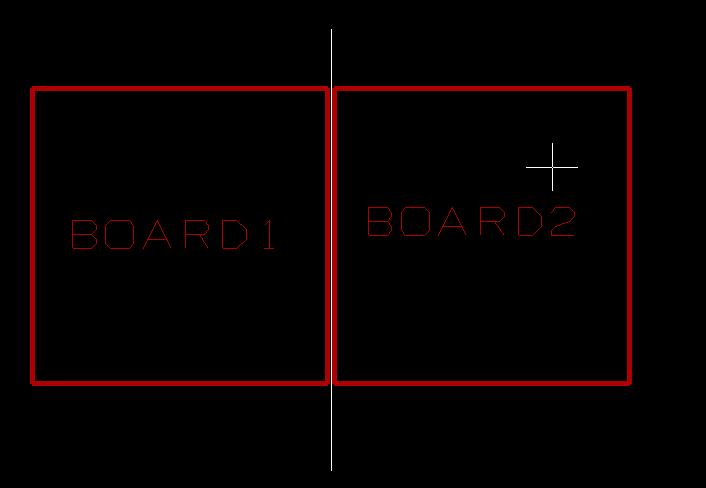
Yes, but we will charge you EUR 5 per each next board on the panel after the first one. i.e. if you send us 3 boards to be panelized in the same panel you will have to pay EUR 10 extra. If you make the panelization yourself there is no panelization charge. When you are sending more than one board file please attach picture how the boards should be panelized. If you do not provide panelization drawing picture we'll try to panelize but will charge you additiona fee. Please reffer our PRICE page for more info. The panelization drawing picture must be in easy viewable format like: BMP, GIF, JPG, PDF and each board on the drawing should have name as the PCB files name you send for it. Please note that we de-panelize the boards from the panel with stright cuts from side to side so this is correct panelization request and this is incorrect panelization request which we can't de-panelize.
No, all boards should have 10 mils borders on all layers (most important on copper layers). If you want your board manufactured without borders we can't de-panelize them and we can ship to you as panel, so you can de-panelize yourself.
No, it may be dashed line, but must be good visible as this is our guide when we de-panelize your boards from the panel
We de-panelize the boards from the panel manually and have two tools for this purpose.
If we assume your board border is 0.254 mm thick (10 mils) and you want guilotinee cut your maximum board dimensions should be 100*79.5 mm or 160*49.5 mm. If you want disk cut your max dimensions should be 100 * 78.75 mm or 160*48.75 mm
For guilotinee cut: X=(160-0.254)/2-0.254 = 79,6 mm Y=(100-0.508)/3-0.254 = 32.9 mm. For disk cut: X = (160-2)/2-0.254 = 78.75 mm, Y = (100-4)/3-0.254 = 31.7 mm
No milling/routing/v-score is available for the prototypes, but these are available for production runs.
FILE FORMATS
NC drill files should be in Excellon or S&M format not in Gerber format.
Please use 2.4 or 3.4 precission.
No, as these formats are not good for PCB manufacturing.
We accept Eagle, Target3001, kiCAD board files. For other CAD products please go to our technical page and read the file generation tutorials, this is no rocket science and easy job so everyone can handle them
GERBERS
Excellent source is available here.
No, please don't send pierced pads gerbers, they look good on your monitor, but are not good for manufacturing.
Composite layer is ancient way to generate your copper pour. This is still used by old CAD software which don't have copper pour hatch stroke filling. Why is bad...pictures
We highly recommend you to check always your generated gerber files with gerberviewer before send them for production. This will save you money (wrongly generated files which lead to production of board with errors) and time we check your gerbers only once per day, so if you submit wrong files we'll report and if you submit new files will check them next working days.
Please don't use under 8 mils line widths in your Gerbers on the copper layers. Basically you can use any line width size to fill your copper polygones, but practice shows that if the stroke width is under 8 mils and the CAD program doesn't generate hatch filling simple stroke to stroke filling the quality of the phototools printed is bad. Many CAD programs have 5 mils or 1 mils line width for copper pour set by default so you have to check your settings as we'll put your order on hold if your copper pour is made with under 8 mils stroke width.
Always export your gerbers in the units you designed board to prevent rounding errors in your Gerber generation due to the unit conversion.
2.4 or 3.4 is OK. Some CAD products have default precision 4.2 or 2.3 which is pretty bad for dense boards as the XY coordinates will be rounded to second digit after the decimal point in first case.
Please use offset 0,0 if you add large offset it will do nothing but make your XY coordinates bigger and there may be errors due to rounding or to exceed maximum number which could be present by the selected the precision.
EAGLE CAD
Welcome to the wonderful wolrd of PCB design :) If you are beginner please follow these steps and you will make perfect boards from the very first time:
Read our TECHNICAL INFO , FAQ and Design Tips web pages before you start your boards
Make your schematic and then route your board, don't route just board without schematic as this is easy way to forget connection or to do something wrong. Once your schematic is correct Eagle will not allow you to route board different than the schematic (i.e. to forget to connect something or to connect it on wrong place)
When you are ready with board routing run 8mils.dru and if there are errors fix them
Postprocess your BRD file to Gerbers and NC drill as written below
Download Gerberviewer from our Design Tools page
Import your files in the Gerberviewer and re-view them carefully
If evrythings looks fine send the generated Gerbers+NC drill or the BRD file to us, don't forget the README.TXT
It's easy. Just do the following steps:
- Open your BRD file and run drillcfg ULP, this will create your "rack" file i.e. drill tool assignment file with extension xxx.DRL (we'll need this file for your PCB manufacturing so don't forget where you saved it)
- See below how to increase the Eagle default drill precision and make the necessary fixes, you need to do this only once
- Run Excellon.cam and process your board with generated DRL rack from the ULP script, this will create xxx.DRD file which keeps XY coordinates (we'll need this file for your PCB manufacturing so don't forget where you saved it)
- Run Gerb274x and Generate gerbers from your board files, it's very important to use Gerb274x not "Gerber" and the latest will not produce correct files, but the obsolete RS274D format (Cadsoft peoples are silly to confuse you so much putting this old stuff on their CAD aren't they?). Gerb274x will create several files from which we need xxx.CMP - your top copper gerber file, xxx.SOL - your bottom copper gerber file, xxx.PLC - your component print gerber file, xxx.STC - your top soldermask gerber file, xxx.STS - your bottom soldermask gerber file
- Zip these files: xxx.CMP, xxx.SOL, xxx.STC, xxx.STS, xxx.PLC, xxx.DRL, xxx.DRD, README.TXT and send to us at fastpcb@olimex.com you will receive PO form with your order confirmation
Do run DRILLCFG.ULP which will extract all drill sizes you are using.
No.We postprocess Eagle BRD files with only default Eagle CAM layers. If you want other layers than defaults please postprocess your BRD file by yourself (see below how).
Eagle put the polygon copper on 8 mils distance by default (when ISOLATE parameter is 0). Use ISOLATE=10-12 mils to increase your copper distance from your pads and tracks.
We just will ignore the Gerbers and process the BRD file, so please decide which files you want to have your board manufactured from and send only Gerbers or BRD..
DESIGN RULE CHECK
We have noticed these phonomens in some cases. They all come from some kind of XY Gerber/NC drill coordinates rounding when the board is designed on the edge of the specs. Possible reasons may be:
you have designed your board in one units, but set your postprocessor to export your Gerbers in other units. for instance designing in metric units but exporting in Inch and vice versa, when the Gerbers are converted from one units to others this may be reason for coordinates rounding errors poor Gerber / NC drill precision: use 2.4 or 3.4 (some CAD products have 4.2 or 2.3 precision set as default option which is not good in all board designs). Increasing the precision makes the files bigger but more precise, the 4.2 and 2.3 formats were much more used in the past when the drill machines couldn't load files bigger than 64KB but now this 8-bit controllers problem doesn't exist, so you have no excuse to not use the more precise formats big XY coordinates, some CADs have option to add "offset" to the 0,0 board origins, this is totally wrong as making the XY coordinates bigger just increase the error from rounding. Move your board near 0,0 origin but do not make it with negative coordinates.


